Keywords
Abstract
This work investigates the effect of low-dose phosphorus ion implantation on the transverse resistance of thin polycrystalline silicon films deposited by low-pressure chemical vapor deposition. The films were implanted with P⁺ ions at 80 keV with doses ranging from 5 to 40 μC/cm2 and subsequently annealed at 900 °C. The samples were characterized by secondary-ion mass spectrometry, transmission electron microscopy, and precision transverse current–voltage measurements. A nonmonotonic dependence of the transverse resistance on the implantation dose is observed: the resistance increases up to a dose of ~20 μC/cm2 and then decreases at 40 μC/cm2. Quantitative analysis within the space-charge-limited current model reveals that the trap distribution parameter l = T0/T increases from 3.8 ± 0.1 for the undoped film to 4.3 ± 0.2 at 20 μC/cm2, indicating a broadening of the trap distribution upon implantation. At 40 μC/cm2, the resistance decreases and the conductivity exceeds that of the undoped film. This behavior is suggested to be due to the competition between implantation-induced defects (which increase trap density and thus resistance) and the activation of phosphorus atoms, which passivate traps and reduce resistance at higher doses. The results provide a guideline for optimizing doping conditions for high-resistance integrated resistors under the specific conditions investigated, particularly for quenching resistors in high-density silicon photomultipliers.
1. Introduction
Polycrystalline silicon (poly-Si) is a key material in modern micro- and nanoelectronics due to a number of its properties, including compatibility with silicon complementary metal-oxide-semiconductor (CMOS) technology and high-temperature process stages, as well as the ability to control the material's resistivity using technological methods. Key applications for poly-Si include the fabrication of:
- gates of high-speed CMOS transistors [1-4];
- active layers of TFT transistors for LCD and OLED displays, as well as flexible and transparent electronics devices [5-7];
- structural layers of MEMS and sensors [8-11];
- electrodes and emitters in silicon solar cells [12-16];
- negative feedback systems in silicon photomultipliers (SiPM) [17-19].
In this paper, poly-Si layers are examined for their use as quenching resistors for SiPMs. Silicon photomultipliers are widely used in lidar, positron emission tomography, flow cytometry, fluorescence spectroscopy, astrophysics, quantum cryptography, and high-energy physics [20]. The high-density silicon photomultiplier (HD-SiPM) contains a significantly larger number of cells compared to the existing design of solid-state photomultipliers, which allows for an increase in the dynamic range of the photodetector without loss of fill factor or increase in the level of correlated noise [21]. HD-SiPM is designed to solve problems of analog detection of short light pulses under high background illumination [22], which is a pressing issue for those modern photonics devices that have the highest demands on the combination of sensitivity, speed, and dynamic range of the photodetector.
A key component of HD-SiPM is a resistor located on the surface of each cell, acting as negative feedback (NFB) and providing passive quenching of the avalanche process for operation in the Geiger mode. In the classical design of a solid-state photomultiplier, a longitudinal configuration of the quenching resistor is traditionally used [17-19], so the overall resistance is determined by the length of the element and the crystallite size. In most cases, longitudinal conductivity is used in the formation of resistors, when current flows through the film, and the resistor resistance is governed by the sheet resistance Rs [Ω/□] and the ratio of the resistor length l to the width d :
However, the reduction in the size of each individual cell in HD-SiPM makes it impossible to use classical avalanche current quenching methods. Implementing a feedback element using a longitudinal resistor requires an extended region in the topology to provide sufficient resistance for efficient cell operation, which imposes strict limitations on its minimum area.
It is worth noting that passive quenching in SiPMs is divided into two fundamentally different approaches: resistive feedback and capacitive feedback (RNFB and CNFB, respectively). When the quenching resistance decreases below a certain threshold, the NFB becomes resistive. This allows for an expanded dynamic range by reducing recovery time, but leads to:
- bandwidth limitation, since in the case of RNFB the recovery of the photodetector cell has only a slow component [23];
- high noise, especially at high gain, since avalanche damping is determined primarily by resistance, and the noise of a resistor is significantly higher than the noise of a capacitor [23];
- proportionality of the output voltage to the instantaneous current, and not to the accumulated charge, the shape of the current pulse will vary greatly [24];
- the possibility of oscillations [23];
- an increase in the probability of crosstalk (correlated triggering of neighboring cells when an avalanche occurs in one of them due to optical interaction), since a large overvoltage is used [23, 24].
For these reasons, СNFB is used for specialized device applications. This is especially relevant for HD-SiPM, where the number of cells can provide sufficient dynamic range to work with background sunlight even with long relaxation times (tens and hundreds of nanoseconds, which СNFB can provide). At the same time, the bandwidth, noise, and pulse shape are important for lidar applications. Consequently, the problem of producing thin, high-resistance semiconductor films for generating NFB in high-density silicon photomultipliers is pressing.
It is known that the use of an undoped semiconductor layer as a negative feedback element in a device leads to nonlinearity of charge transfer due to the formation of potential barriers around grain boundaries [25, 26], and consequently to various problems in the operation of a silicon photomultiplier (increased cell recovery time, residual charge on the quenching layer under conditions of high illumination intensity, deterioration of detector sensitivity).
The sheet resistance of doped polycrystalline silicon films typically does not exceed a few kΩ/□; therefore, high-resistance resistors are fabricated using very large l/d values. In this case, the area occupied by the resistor is quite large, which may hinder the increase in device integration density. It is advisable to consider the possibility of exploiting the transverse conductivity of the films, where the current flows normally to the film plane, and the resistance is proportional to the resistivity ρ and the film thickness d and inversely proportional to the cross-sectional area of the structure s:
For use in CNFB, films with a sufficiently high resistance (from 1 to 10 MOhm with a thickness of about 0.5 μm and a resistor cross-sectional area of about 10 μm2) are of interest. For this, the resistivity of the film should be from 2 to 20 kOhm·cm. Such high resistivities can only be characteristic of lightly doped or undoped polycrystalline silicon films [27, 28]. The conductivity of thin polycrystalline silicon films is usually described by the space-charge-limited current (SCLC) model with an exponential distribution of volume traps by energy in the band gap [29, 30], which is confirmed by optical [31] and electrophysical [32-41] research methods.
Traditionally, in-situ doping of LPCVD-deposited polycrystalline silicon is used [42, 43], which allows achieving high concentration uniformity over depth without the use of high-temperature annealing, which can affect the crystalline structure of the film. However, the limited applicability of in-situ doping technology due to economic factors (high cost of equipment and its maintenance under conditions of partial loading of production capacities, expensive and hazardous reagents) makes it necessary to search for an alternative doping method, which is ion implantation (despite the high cost of equipment, it is often a more advantageous technological solution due to its versatility). Studies of the effect of ion implantation dose on the conductivity of LPCVD polycrystalline silicon films have been conducted previously [44], but for the longitudinal configuration, while systematic studies of transverse conductivity are practically absent, which determined the direction of this work.
The aim of the work is to establish a correlation between the phosphorus implantation dose (in the range of 5–40 μC/cm2) and the transverse resistance of thin LPCVD poly-Si films, and to identify the physical mechanisms responsible for the nonmonotonic resistance behaviour. Particular attention is paid to the role of implantation-induced defects versus dopant activation, and to the contribution of grain boundaries and contact effects to the overall transport.
2. Methodology
The transverse resistance of the poly-Si films was determined by analyzing their current-voltage characteristics (I–V). Seven wafer samples with films obtained under various process parameters (annealing temperatures and dopant concentrations), as well as a control wafer designed to measure the poly-Si thickness and dopant distribution (Table 1), were analyzed on a PEGASUS S200 probe station using a Keithley 236 source-measure unit.
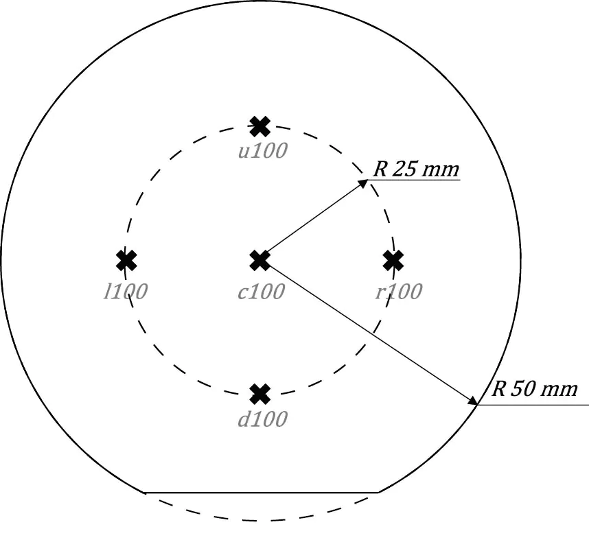
Titanium contact pads with a diameter of 100 µm were deposited on five areas of each wafer: at the geometric center of the wafer, excluding the base cut, and at a distance of 25 mm from it in four directions. The schematic layout and symbol for each pad are shown in Figure 1.
It is known that the decisive contribution to the electrophysical properties of a polycrystalline material film is made by grain boundaries, namely their size, orientation, width of the intercrystalline space, and the presence of foreign impurities (O2, C, N2, H2) [45-49]. Critical parameters of the LPCVD deposition process of polysilicon include temperature, pressure, composition of the process gas, and concentration of dopant elements [9, 50-54]. Residual mechanical stresses in the deposited polysilicon films can be controlled by changing the deposition temperature and pressure, as well as the parameters of subsequent annealing.
In the experiment, LPCVD deposition of polysilicon was carried out at a temperature of 620 °C, which is sufficient to form a thin film with a columnar structure that has good stability and reproducibility [52-56].
The annealing temperature was varied in the study: one of the wafers was annealed at 1000 °C, 4 wafers were annealed at 900 °C, and one wafer was not annealed in order to study the effect of residual mechanical stresses on the transverse resistance of the film. The holding time for all annealings was 10 min. Temperatures below 900 °C do not have a significant effect on internal mechanical stresses [57], while increasing the annealing temperature above 1000 °C can lead to a significant increase in the static resistance of the film in the absence of mechanical stresses and a sharper dependence of the resistance on stress, since the influence of defects increases [58, 59]. It should be noted that the effects reported in [58] are primarily microstructural in nature – they are related to grain growth, defect relaxation, grain boundary transformation, and stress relief that occur during high‑temperature annealing above 1000 °C [12]. Although that work was performed on boron‑doped poly‑Si films, these microstructural transformations are universal for polycrystalline silicon and do not depend on the specific dopant type. Therefore, the conclusions of [58] are used here to support the general statement that annealing above 1000 °C significantly alters the defect structure and, consequently, the resistance of poly‑Si films. In addition, it is known from literature sources [59, 60] that a temperature of 900 °C should be sufficient for uniform distribution of phosphorus over the depth of the poly-Si (400 nm).
Phosphorus doping doses were varied from 0 to 40 μC/cm2 to study the effect of impurity concentration on the transverse resistance of the resulting polycrystalline silicon film. The implantation energy of 80 keV was chosen because it is a standard value for doping thin poly-Si films, providing a controllable introduction of dopants and defects without causing amorphization. According to SRIM simulations, the projected range of 80 keV P⁺ ions in silicon is about 95 nm, with a straggling of ~40 nm. Although the poly-Si film thickness in our study is 400 nm, the ion penetration depth is sufficient to create a substantial defect population in the near-surface region (down to ~130 nm). During the subsequent annealing at 900 °C, both the implanted phosphorus and the generated point defects can diffuse, influencing the electrical properties throughout the entire film thickness. Thus, this energy allows us to study the effect of implantation-induced defects on the transverse resistance, which is sensitive to defects in all parts of the film, especially near the interfaces where the electric field is concentrated in the transverse measurement configuration.
The differential resistance dependences on voltage were obtained by measuring direct current-voltage characteristics. Measurements were performed using a Pegasus S200 probe station and a Keithley 236 source-measure instrument. A positive potential was applied to the film contact pads using the probe. The stage on which the wafer was placed was connected to ground. Thus, by measuring steady-state current-voltage characteristics, the transverse resistances of the poly-Si film were obtained at different applied positive voltages.
Using time-of-flight secondary ion mass spectrometry (SIMS) on an ION-TOF ToF.SIMS 5–100 system, the dopant distribution profile within the film bulk and the concentration of dopant atoms were determined. Depth profiles were calibrated using ion etch crater measurements with a Tencor AlphaStep 200 profilometer.
Transmission electron microscopy (TEM) was used to study the grain structure of the poly-Si film (grain size, shape, and orientation). Sample preparation for TEM was performed using a focused ion beam. The TEM study was performed only on wafer N1 with a film obtained at a deposition temperature of 620°C without doping or post-growth annealing.
3. Results and discussion
3.1. Transmission electron microscopy
TEM was performed only on the undeposited, non-implanted, and unannealed sample N1 to verify the typical columnar microstructure of the as-deposited LPCVD poly-Si film. For the implanted and annealed samples, we rely on extensive literature data [52, 61-63] showing that annealing at 900 °C does not significantly change the grain size in thin LPCVD poly-Si films, but mainly affects the defect density within grains. Therefore, the observed electrical changes are attributed to the implantation-induced defects and dopant activation rather than to morphological alterations.
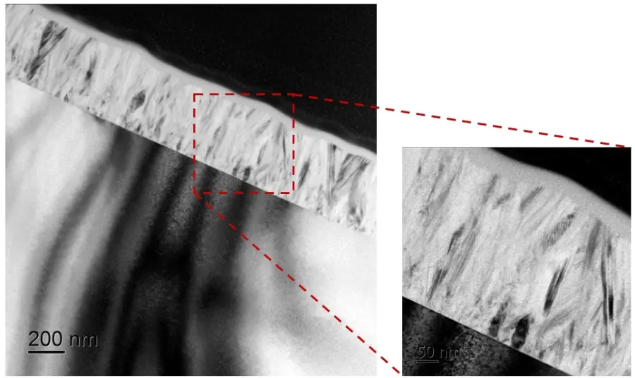
TEM studies revealed that the film thickness ranges from 320 nm to 400 nm, averaging 350 nm. The crystallites have a columnar cone-shaped structure, with cone diameters of 10–30 nm near the substrate and either decreasing or increasing toward the surface, most often at an angle of approximately 30°. Thus, the transverse grain size near the surface can be 50–100 nm (Figure 2). A large number of crystalline twins are observed in the bright field, making grain boundaries visible only in the dark field (Figure 3). Consequently, the thickness of the intercrystalline space cannot be measured with high accuracy using this method and on this wafer.
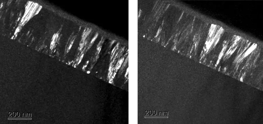
From the light and dark field images, it is possible to determine the preferred directions of grain boundaries (see Figure 3, dark field) and twinning boundaries (see Figure 2, light field and Figure 3, dark field) – this is the direction parallel to the normal to the substrate {100}, and directions located at an angle of approximately 30°.
Figure 4 shows an electron diffraction pattern for a polycrystalline silicon film, from which we can determine the intensity of the diffraction rings. It is evident that, besides the central reflection, only the first ring is clearly distinguishable, while the next two contribute significantly less. This agrees well with the angles measured in the TEM image, since the first ring represents the {111} plane, located at an angle of 28.5°. Furthermore, the electron diffraction pattern reveals a large number of artifacts associated with twinning in the polycrystalline film. These artifacts manifest themselves as double or elongated reflections symmetrical about the central axis, as well as the appearance of reflections uncharacteristic of silicon {100}.
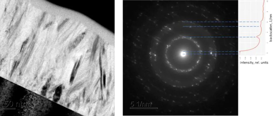
Thus, the grains are columnar and cone-shaped, with grain boundaries predominantly aligned with the substrate normal {100} and in the “adjacent” most densely populated crystallographic plane {111}. Twinning planes obey the same laws. The size of the intercrystalline space is difficult to accurately estimate due to twins and the presence of small crystallites. The electron diffraction pattern is more reminiscent of that of coarse-grained silicon (an average crystallite size of ⪆50 nm is sufficient for this) due to distinct individual reflections on the rings. However, at the same time, high intensity is observed between the rings, which is characteristic of amorphous Si.
3.2. Secondary ion time-of-flight mass spectroscopy
Secondary ion mass spectrometry (SIMS) measurements were performed in negative secondary ion mode by sputtering the surface with 2 keV Cs+ ions. The sputtering crater size was 150 × 150 μm, and the analysis was performed in its central region, measuring 50 × 50 μm2, using a 30 keV Bi⁺ beam.
The measured data were converted into concentration profiles for the corresponding elements (Figure 5). Data on the average phosphorus concentration and dose are presented in Table 2.
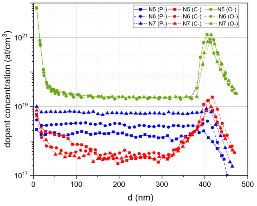
Overall, the measured dose values are in very good agreement with those used in the experiment. It is also noticeable that the carbon and oxygen concentrations and their depth distribution are identical for all three films measured.
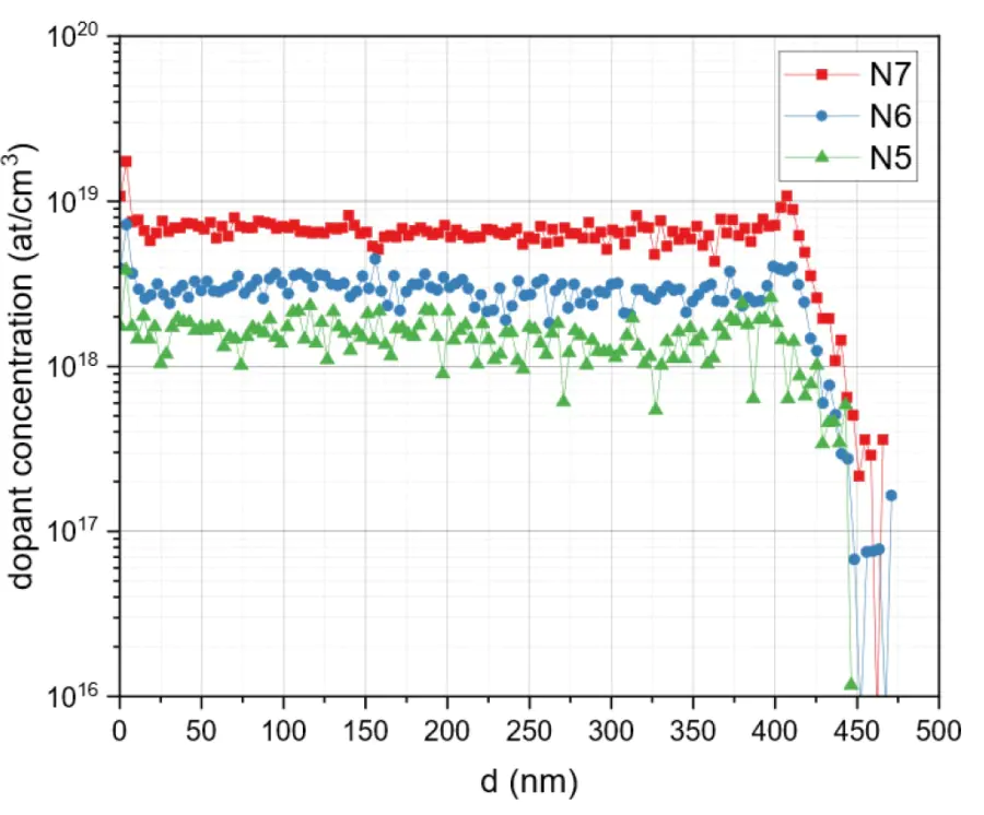
For ease of comparison, the phosphorus profiles for the different samples are presented in the same coordinate system in Figure 6. It is also worth noting that the main difference between the films lies only in the phosphorus profile.
3.3. I–V characteristics
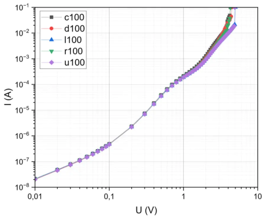
Probe measurements of steady-state I–V characteristics were carried out on wafer N1. The measurement results are presented in Figure 7. The designation in the legend is the point on the wafer at which the measurement was performed (see Figure 1).
Measurement mode:
- From 0 V to 0.1 V – in 0.01 V increments, holding time of 1 s per point,
- From 0.1 V to 10 V – in 0.1 V increments, holding time of 1 s per point,
- Current limit – 100 mA.
The graph clearly shows high wafer-to-wafer reproducibility on 100 µm Ti contact pads. Differences are observed only in the voltage range above 2-3 V, which is explained by the electric field strength approaching the breakdown value for the transverse configuration of the poly-Si thin film.
3.4. Dependence of resistance on applied voltage
The obtained data were converted into differential resistance. The dependence of transverse resistance on applied voltage is shown in Figure 8.
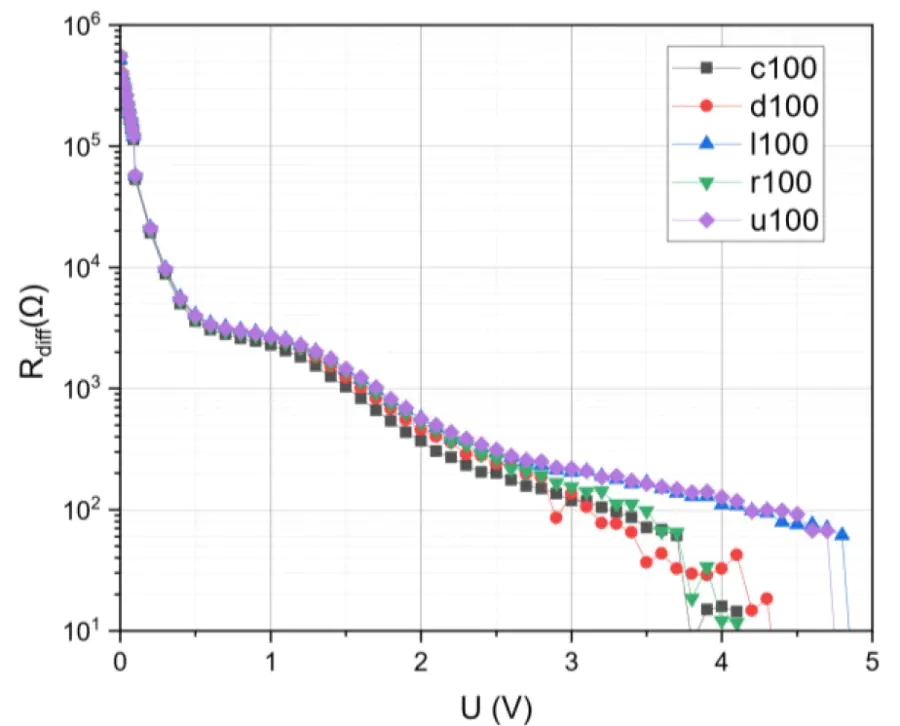
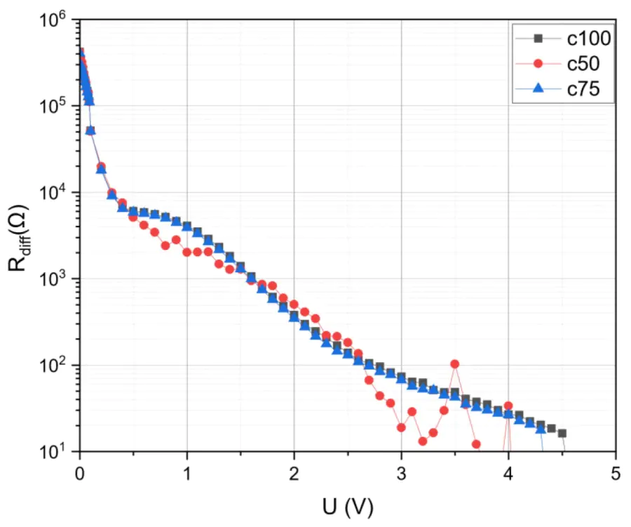
The previously noted high reproducibility of the current on 100 µm contact pads across the wafer is observed in all the obtained samples; for this reason, Figure 9 and Figure 10. show only the average values of Rdiff(U) for all the obtained films.
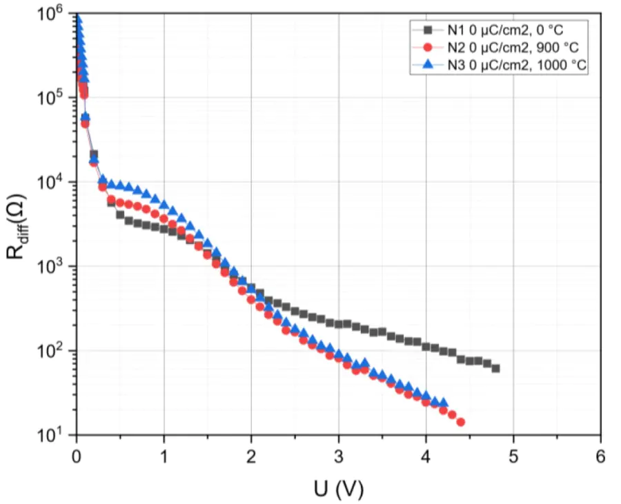
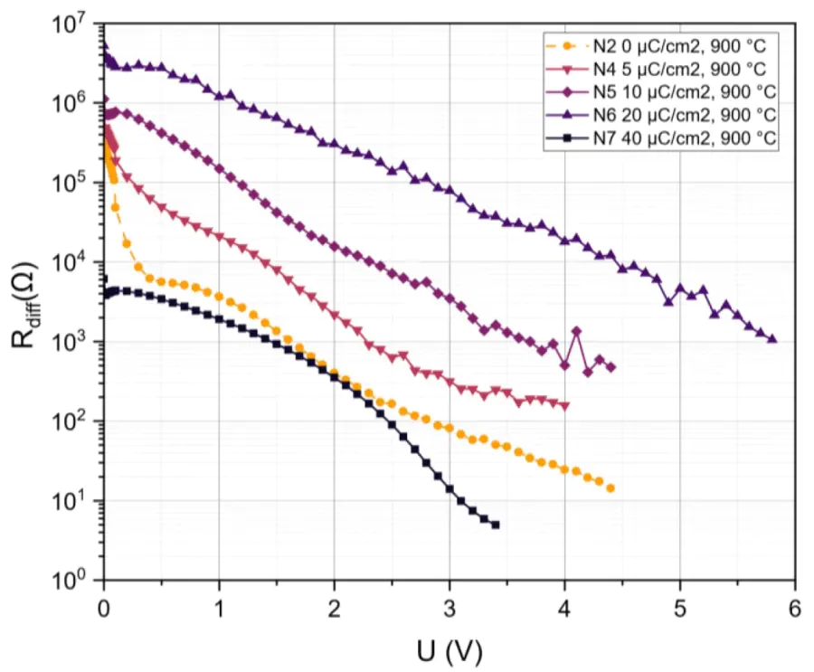
The dependences in Figure 10 demonstrate that annealing at 1000°C has little effect on the electrical behavior of undoped polysilicon thin films, slightly altering the slope of the curve and the positions of its inflections. Doping dose significantly influences R(U): the resistance increases, on average, with increasing doping dose from 0 to 20 μC/cm2, then begins to decline, and, furthermore, the initial inflection begins to disappear.
To separate contact effects from bulk film resistance, we performed additional measurements on contacts with diameters of 50, 75, and 100 μm in the center of the wafer. The results in Figure 9 show that at voltages below 0.5 V, the current scales sublinearly with contact area, indicating the dominance of a Schottky-type barrier at the Ti/poly-Si interface. Above 0.5 V, the current scales linearly with contact area, confirming that the bulk film resistance dominates and the SCLC model is applicable. The equivalent circuit of the transverse measurement structure can thus be represented as a series combination of two back-to-back Schottky diodes (representing the Ti/poly-Si interfaces) and the bulk poly-Si film resistance. The Schottky barrier height, estimated from the low-voltage region using thermionic emission theory, is 0.65 ± 0.05 eV, which is consistent with the reported work function difference between Ti (4.33 eV) and moderately doped n-type silicon (electron affinity ~4.05 eV). The extraction of SCLC parameters was performed on the linear scaling region (U > 0.5 V), ensuring that the extracted trap parameters reflect the bulk properties rather than contact artifacts.
3.5. Physical interpretation of the results
The shape of the I–V curve in Figure 7 is qualitatively similar to the current–voltage characteristic of a film whose conductivity is described by the space-charge-limited current (SCLC) conductivity model with an exponential distribution of bulk traps distributed in energy within the bandgap, which is typical for polycrystalline films [30] and poly-Si films in particular [29]. One of the key assumptions of the model is a uniform distribution of traps in the film bulk. However, despite the fact that the morphology of the studied polysilicon films (the grain size in the transverse direction reaches the film thickness) suggests a dominant role of traps at grain boundaries, it was experimentally found that the current–voltage characteristics are qualitatively described by the bulk SCLC model. Thus, the electrophysical properties of the film can be qualitatively described by the SCLC model in the homogeneous approximation.
Although the films are polycrystalline with columnar grains, the SCLC model assumes a uniform trap distribution, which may correspond either to bulk traps within grains or to grain boundary traps if the grain size is small enough. In our case, TEM shows that the grain size in the transverse direction is 50–100 nm, comparable to the film thickness. This suggests that grain boundaries may indeed play a significant role. However, the high density of twins (observed in TEM) and the presence of small crystallites make it difficult to separate grain boundary and bulk contributions. We attribute the observed resistance increase to implantation-induced defects, which are likely distributed both within grains and at grain boundaries, with the latter being particularly important in polycrystalline films [45-49]. Future work is needed to quantitatively distinguish these contributions.
In this case, the difference between the dependences of the transverse resistance of the polysilicon films on the diffusion annealing temperature, shown in Figure 10., is explained by the difference in grain size and grain boundaries. With the introduction of annealing into the process or an increase in its temperature, an increase in the size of polysilicon grains should be expected, which reduces the overall trap density and changes the trap energy distribution pattern due to the redistribution of dangling bonds at grain boundaries. Conductivity at voltages U < 0.5 V is most likely limited by thermal emission over the Schottky barrier. The Schottky barrier is formed at the Ti/poly-Si interface. With a Ti work function of 4.33 eV and silicon electron affinity of 4.05 eV, the expected barrier height is approximately 0.65 eV, which is consistent with our estimate of 0.65 ± 0.05 eV extracted from the low-voltage region using thermionic emission theory. This confirms that the low-voltage conduction (U < 0.5 V) is indeed limited by thermionic emission over this barrier. At higher voltages, shallow traps, which quickly fill upon application of voltage, play a key role in charge transport in the unannealed sample. Thus, the N1 film has a relatively narrow trap energy distribution with a high characteristic distribution constant. Annealed films have a smaller number of shallow levels, and ordered dislocation defects with deep energy levels play a greater role in charge transport.
The SCLC model also allows for a qualitative interpretation of the dependence of the transverse resistance of poly-Si films on the presence and varying doping doses, as shown in Figure 11. The R(U) plot for the undoped N2 film exhibits a pronounced inflection in the voltage range up to 0.5 V. For doped films, the inflection is less pronounced, since doping of the near-contact region lowers the Schottky barrier and facilitates charge carrier tunneling, and the conduction mode quickly switches to the SCLC. The plot shows that the transverse resistance of the film increases, on average, with doses from 0 to 20 μC/cm2, as noted separately in Figure 12. Figure 12 presents the transverse resistance values averaged over five contact pads per wafer, with error bars representing the standard deviation. The error bars represent the standard deviation of the mean and are voltage‑dependent due to the non‑linear I–V characteristics. The undoped sample already exhibits a noticeable irreproducibility across the contact pads, with relative uncertainties ranging from ±10 % at low voltages to ±25 % at high voltages, likely due to residual stress and growth‑related defect non‑uniformities. The introduction of low implantation doses (5 μC/cm²) further increases the scatter: from ±12 % to ±40 %. This behaviour indicates that ion implantation creates a spatially non‑uniform defect distribution at low doses, where the defects are not yet compensated by activated dopants. In contrast, the 20 and 40 μC/cm² samples show the smallest scatter, with uncertainties between ±5 % and ±15 % across the entire measured range, reflecting the homogenisation of electrical properties due to trap passivation (at 40 μC/cm2) or trap saturation (at 20 μC/cm2). The error analysis confirms that the resistance increase from 0 to 20 μC/cm2 and the subsequent decrease at 40 μC/cm2 are statistically significant at all voltages. The most likely cause of this behavior appears to be the creation of traps during ion implantation. Ions with an energy of 80 keV knock out silicon atoms, creating both interstitial atoms and dislocations, which are not completely eliminated during annealing. At doping doses below the threshold, the amount of active impurity is insufficient, and the defect-forming effect of ion implantation dominates over the doping effect. Above this dose (40 μC/cm2 in the experiment), the concentration of impurity atoms becomes sufficient to passivate traps in the bandgap with free carriers, and the film conductivity increases.
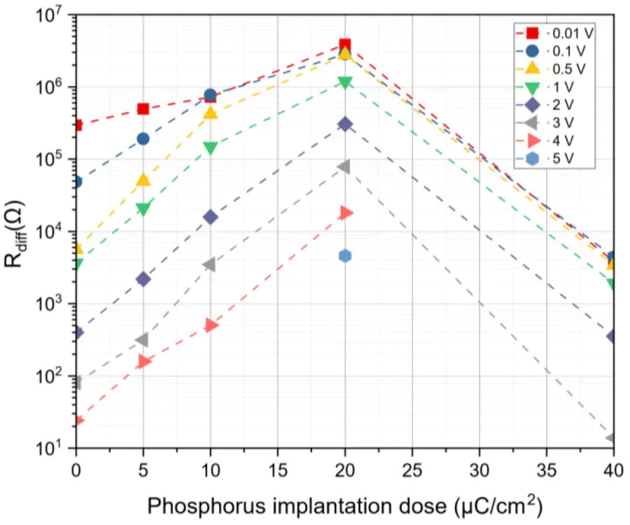
The dose range between 20 and 40 μC/cm2 was intentionally chosen with a larger interval to bracket the expected threshold behavior while minimizing the number of wafers processed in this exploratory study. Based on preliminary experiments and literature data [64], we anticipated that the transition from defect-dominated to dopant-dominated conduction would occur between 20 and 40 μC/cm2. The experimental data confirm this expectation, showing a clear resistance decrease at 40 μC/cm2. However, we acknowledge that the exact shape of the R(dose) curve between 20 and 40 μC/cm2 is unknown; therefore, we present the data as discrete experimental points without connecting lines, as shown in the revised Figure 12.
To provide quantitative support for the SCLC interpretation, we extracted the key trap parameters from the I–V characteristics using the standard model for a single-carrier SCLC with an exponential trap distribution [30]. In this model, the current density J is related to the voltage U by J ∝ Ul+1, where l = T0/T, with T0 being the characteristic temperature of the exponential trap distribution and T the measurement temperature. The extracted values of l increase from 3.8 ± 0.1 for the undoped film to 4.3 ± 0.2 for the 20 μC/cm2 sample, indicating a broadening of the trap distribution upon implantation. Correspondingly, the total trap density Nₜ, estimated from the transition voltage Utrans between the Ohm's law regime and the SCLC regime, shows a maximum at 20 μC/cm2, consistent with the resistance maximum observed in Figure 12. The transition voltage Utrans increased from 1.6 ± 0.1 V for the undoped film to 2.5 ± 0.2 V for the 20 μC/cm2 sample, confirming that ion implantation introduces additional trapping states that must be filled before space-charge-limited conduction can dominate. These quantitative parameters are summarized in Table 3. The decrease in resistance at 40 μC/cm2 is accompanied by a reduction in T₀ and Nₜ, which we attribute to the passivation of implantation-induced defects by activated phosphorus atoms.
At 40 μC/cm², the activated phosphorus concentration (~6.6×10¹⁸ at/cm³) is sufficient not only to passivate the implantation-induced traps (point defects and dislocation loops) by filling them with free carriers, but also to contribute excess carriers that increase the conductivity above that of the undoped film (see Figure 12). This indicates that the doping effect dominates over the residual defect scattering at this dose. In contrast, at 20 μC/cm2, the number of activated donors is still insufficient to compensate the defect-induced traps, resulting in a maximum resistance (minimum conductivity). Thus, the nonmonotonic behaviour arises from a crossover between defect-dominated and doping-dominated conduction, with the threshold near 20 μC/cm2.
In Macdonald et al. (2003) [64], the authors investigated the effect of the Si+ ion implantation dose in single-crystal silicon and the subsequent annealing temperature on the charge carrier lifetime. The study concluded that ion implantation with a dose of 1014 ions/cm2 (approximately corresponding to 20 μC/cm2 in this experiment) leads to a decrease in the charge carrier lifetime due to the formation of surface defects, and an annealing temperature of 900 °C is insufficient to reduce the defect concentration, unlike 1000 °C.
Recent modeling and experimental studies by Fırat et al. (2022) [65] have shown that phosphorus diffusion from poly-Si films into the underlying silicon during annealing is significantly enhanced in the vicinity of structural defects (such as pinholes in the interfacial oxide). This results in semicircular regions of locally increased doping concentration extending deep into the silicon. Although their study focused on poly-Si passivating contacts with a thin interfacial oxide, this work directly confirms that phosphorus atoms diffuse over appreciable distances (~several hundred nanometers) from the poly-Si film during annealing at 900°C. This provides direct support for our interpretation that phosphorus atoms implanted at 80 keV (projected range ~95 nm) can diffuse throughout the entire 400 nm film thickness during the 900°C anneal, effectively passivating traps and reducing the resistance at the highest dose of 40 μC/cm2.
Also, earlier, Matsumura et al. (1980) [66], conducted a study of the effect of ion implantation dose on the resistivity of amorphous silicon obtained by hydrogenation sputtering, and also searched for optimal annealing conditions to minimize defects introduced by the implantation process. The work found that phosphorus doses up to 1016 ions/cm2 do not increase the conductivity of the material at room temperature, while doses of 1014-1015 ions/cm2 can reduce it.
Conclusion
It was found that an undoped and unannealed poly-Si film obtained by LPCVD deposition at 620 °C has a high density of crystalline twins, which prevents direct measurement of grain cross-sectional geometric parameters. The nature of the twinning is likely related to high residual mechanical stresses in the film. A presumed cause is the LPCVD process temperature, close to the formation regime of amorphous Si, combined with the absence of post-growth annealing.
Ion implantation of the poly-Si film with 80 keV phosphorus atoms results in a nonmonotonic dependence of the film's transverse conductivity on the doping dose. Experimentally, a decrease in the transverse conductivity of the film at room temperature is observed as the dose increases up to 20 μC/cm2 (1.3 · 1014 ions/cm2), as carrier scattering and trapping at surface defects, which are not eliminated even by annealing at 900°C, dominate over the doping effect. This dose of 20 μC/cm2 is a “threshold”, and at 40 μC/cm2 (2.9 · 1014 ions/cm2), the impurity atom concentration becomes sufficient to passivate traps in the bandgap with free carriers, and the film conductivity increases.
For the specific experimental conditions investigated – LPCVD poly‑Si films with thickness of 350–400 nm deposited at 620 °C, phosphorus ion implantation at 80 keV, and subsequent annealing at 900 °C for 10 min – the threshold dose of 20 μC/cm2 represents the minimum dose required to observe a transition from defect‑dominated conduction to dopant‑dominated conduction. This dose marks the boundary below which ion‑implantation‑induced defects degrade the transverse conductivity, and above which activated phosphorus atoms begin to passivate traps and enhance conductivity. However, the precise threshold value is expected to depend on the film thickness, deposition temperature, annealing conditions, and contact geometry. Therefore, the reported threshold should be considered as a guideline for similar process conditions rather than a universally applicable optimum.
Acknowledgments
The authors express their gratitude to Zelenograd Nanotechnology Center JSC for depositing thin films of polycrystalline silicon using the LPCVD method in accordance with the submitted technical specifications, as well as to the National Research University Moscow Institute of Electronic Technology for conducting secondary ion mass spectrometry on the obtained samples.
References