Keywords
Abstract
This paper describes the fabrication technology and design of the developed monolithic semiconductor position-sensitive detectors. A distinguishing feature of these structures is their small pixel size (approximately 15 × 15 μm). The results of experimental studies of the detectors are presented, including measurements of the electrical characteristics of the fabricated semiconductor structures in the form of bare dies of semiconductor ICs and an analysis of the uniformity of the detectors’ sensing arrays using laser irradiation. The advantages and disadvantages of the developed detectors are compared with those of commercially used position-sensitive detectors. A method based on focused laser irradiation in the two-photon absorption regime was proposed and tested on the developed detectors to investigate the depth of regions sensitive to ionizing radiation. Factors affecting estimates of the sensitivity of semiconductor structures obtained using focused laser irradiation in multiphoton absorption regimes are discussed.
1. Introduction
1.1. Applications of position-sensitive detectors of ionizing radiation
The development and use of pixelated position-sensitive detectors are important in various fields of science, technology, and industry. Demand for these devices is driven by their ability to detect the passage of a particle, measure the energy transferred to the material, and determine the coordinates of the interaction with high spatial precision.
Their main applications include:
– Applied physics research involving particle accelerators. Silicon pixel detectors are used in the tracking systems of modern colliders. For example, they serve as detector elements in the ATLAS and ALICE experiments at CERN’s Large Hadron Collider [1-3]. Similar detector systems are also needed in controlled thermonuclear fusion projects, such as the International Thermonuclear Experimental Reactor (ITER) [4], where they can be used for plasma diagnostics and neutron-field monitoring. They are also used in numerous laboratories worldwide that operate charged-particle accelerators for various purposes [5].
– Monitoring radiation conditions on Earth and in space. Because these devices can determine exposure levels in real time, they are often used to study variations in the fluxes of particles in space [6, 7].
– X-ray diffractometry and microtomography. X-ray diffractometers use these detectors to analyze the crystal structure of materials. Microtomographs use them to obtain three-dimensional images of the internal structure of samples at micrometer resolution without physically damaging the samples [8, 9].
– Medical applications. As radiotherapy and diagnostic radiology develop, pixel detectors are becoming an important component of medical equipment. They are used in so-called “color” X-ray imaging, which offers new possibilities for tissue characterization and functional diagnostics [10, 11].
1.2. Design principles of modern position-sensitive detectors
Semiconductor detectors of ionizing radiation can be divided into two main categories [12-15]: monolithic and hybrid detectors.
Hybrid detectors consist of more than one die. Examples include flip-chip pixel detectors, in which a die containing the detecting pixels is joined to a die containing signal-processing and amplification circuits. Scintillation detectors may also be classified as hybrid because they contain a separate scintillator component.
One of the main technological and economic disadvantages of hybrid detectors is the complexity and high cost of hybrid integration, specifically the formation of reliable, uniform fine-pitch bump bonds. Although bump bonding has been widely used since the 1970s, it remains an expensive manufacturing step that requires precision equipment and substantially affects the final cost of the detector [16]. Hybrid detectors also have significant practical advantages: they can incorporate more complex signal-processing circuits than monolithic detectors, and the sensing array can be selected for a particular application while retaining the same signal-processing system.
Monolithic detectors are devices fabricated on a single die. The die contains both elements sensitive to the radiation being detected (strips or pixels) and signal-processing circuits. Despite the advantage of using a common fabrication process for the detecting pixels and their signal-processing circuits, the development and manufacture of monolithic detectors present several significant challenges [17, 18]: the dopant concentrations in the detector pixel regions and the signal-processing regions differ by orders of magnitude, and the individual blocks on the die must be isolated.
Detector pixels may be based on various structures, including p–i–n diodes, avalanche diodes, bipolar transistors, and metal–insulator–semiconductor (MIS) structures. Regardless of the structure used, the principles of signal processing are similar: each pixel has its own amplification and signal-processing circuitry, which identifies its row and column and provides other functions such as information storage, readout, and reset [19].
To perform these functions, signal-processing circuits may include cascaded and differential amplifiers implemented using either bipolar or complementary metal–oxide–semiconductor (CMOS) technology. RC filters or other filters containing capacitors may be used for filtering [20]. Information may be stored in circuits containing capacitors or by means of flip-flops. More complex signal-processing systems may include memory cells, such as first-in, first-out (FIFO) memory for the sequential output of pixel signals, to store and output information.
1.3. Current state of the development and use of position-sensitive detectors
The applications described above indicate a need for compact, cost-effective solutions for radiation imaging. In particular, the development of monolithic detectors capable of operating in the low-energy X-ray range remains relevant. The growing number of companies manufacturing such devices supports this assessment. Companies specializing in multi-element detectors for X-ray detection and imaging include Dectris (Switzerland), Ideas (Norway), X-Spectrum (Germany), ASI (the Netherlands), PiTec (Brazil), Direct Conversion (Sweden), Advacam (Finland and the Czech Republic), and Quantum Detectors (the United Kingdom). Their products use both sensors supplied by other manufacturers and sensors developed in-house, as well as licensed integrated circuits from the Medipix and Timepix families developed at CERN.
During the development of the chips studied in this work, the state of the art and development trends were reviewed. This review indicated that developing a monolithic sensing array for quantum position-sensitive detectors of ionizing radiation with a spatial resolution of 15 μm remains relevant, since no complete match was found between the distinguishing features of the proposed design and those of existing patented designs. Table 1 presents part of this analysis by comparing the developed chip with the Medipix and Timepix devices most commonly used by manufacturers [21-36].
This paper describes prospective monolithic semiconductor quantum detectors with surface LOCOS isolation. The detector design parameters were determined from the modeling performed in [21], which aimed to optimize the structure for detecting photons with energies of 4–20 keV. The fabricated structures can also detect other types of radiation, including infrared laser radiation, as demonstrated in this work and in [37]. Results are presented from tests of monolithic detector chips based on arrays of silicon p–i–n diodes and from experimental sensing arrays fabricated using a similar process. In particular, statistical data on the electrical characteristics of experimental 256 × 256-pixel sensing arrays are presented. A method for investigating the structure of semiconductor devices using a focused laser source operating in the two-photon absorption regime was also proposed and experimentally tested on the developed detectors. The depth dependence of the detector response was compared with the calculated focal position and the space-charge region.
2. Design of the developed detectors
2.1. Pixel parameters of the developed detectors
Figure 1 shows the design of the developed structures as a cross section of the die in the sensing array region. The substrate is made of phosphorus-doped silicon (KEF-4000). The sensing elements are pixels based on silicon p–i–n diode structures, with two diodes in each array pixel. The p+ regions were formed by boron doping. Individual array pixels are isolated at the surface using LOCOS (local oxidation of silicon). The back surface of the substrate was additionally doped with phosphorus to form an ohmic contact. Two metallization levels were formed to enable the pixel coordinates to be determined by row and column.
Each diode in the sensing array has the following geometrical parameters: p+ region depth of approximately 1 μm (base depth); p+ strip width of approximately 3.75 μm (base width); spacing between pixels of approximately 1.5 μm; and pixel size of approximately 15 μm.
Two types of fabricated detector structures are considered in this study: sensing-array specimens and specimens of monolithic pixel detectors. In addition to the diode sensing arrays, the detectors have a digital signal-processing system on the die, as shown in Figure 5. The pixel parameters are identical in the two types of specimens.
2.2. Sensing-array test specimens
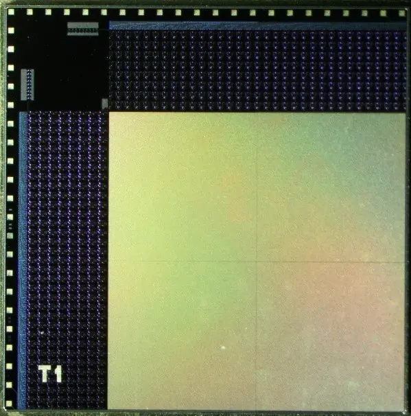
The sensing-array test specimens contain four segments, each containing a 256 × 256-pixel array. A photograph of a die is shown in Figure 2.
In the sensing-array test specimens, the pixels are grouped into segments according to the schematic diagram shown in Figure 3.
The sensing-array die measures 9850 × 9850 μm. The outputs of the pixels within each of the four segments are interconnected in the layout and routed to the corresponding contact pads:
− Segment No. 1 – contact pad 1;
− Segment No. 2 – contact pad 2;
− Segment No. 3 – contact pad 42;
− Segment No. 4 – contact pad 43.
Figure 4 shows an optical microscope image of the pixels in the position-sensitive structure.
2.3. Monolithic pixel detector test specimens
The test specimens of monolithic pixel detectors are structures that allow the detection of irradiation of individual pixels. They comprise a detector section and a section that processes the detector signals. The structure includes:
− a diode array of 64 × 64 pixels;
− current sources required to power the signal-processing elements;
− amplifiers for signal amplification. The activation threshold of the amplifiers is adjusted by an external resistor;
− decoders that convert signals from the 64 columns and rows into digital output signals;
− output stages designed to increase the rise and fall rates of the signals from the decoders.
The die of the monolithic pixel detector measures 3700 × 3700 μm. A photomicrograph of an experimental test specimen is given in [37].
A schematic cross section of the structure is shown in Figure 5. The parameters of the fabrication layers are given in Table 2. As noted above, the sensing pixels of this structure are identical to those of the sensing-array structure. The signal-processing section is a CMOS structure comprising amplifiers, row and column decoders, and current sinks. Bulk isolation of the sensing array from the signal-processing section is provided by a reverse-biased p–n junction; surface isolation is provided by a LOCOS layer.
The authors consider it necessary to note that the monolithic pixel detector structures served as test specimens in the experiments reported in [37]. The specimen connection scheme and the PULSCAN PULSYS-RAD system used in that study were also similar to those used here. Nevertheless, the authors consider the results reported in [37] and in the present work to warrant separate publications for the following reasons:
1) One of the main difficulties in studying the effects of laser irradiation on semiconductor devices is insufficient information about the devices under study: whether coatings are present on the die and what their optical properties are, and how the metallization and semiconductor layers are arranged. Consequently, for a device that is effectively a “black box,” some coefficients describing its optical properties become fitting parameters. The detectors used in [37] were selected because the authors needed devices known to have no extensive multilayered bulk metallization and to have discrete elements of known dimensions. The latter is essential for studying the dependence on beam size considered in [37]. The description of the detectors in [37] was deliberately limited to information about how irradiation responses arise and are recorded, which was relevant to the discussion of radiation testing. A more detailed description of the experimental structures would have shifted the focus of that study. The present work provides a comprehensive description of the detector fabrication technology and describes the sensing-array test specimens for the first time.
2) The aim of [37] was to investigate how the results of scans with focused beams depend on beam size for semiconductor structures whose design rules are close to the beam size. Thus, other devices meeting these criteria – for example, memory ICs or programmable logic ICs – could have been used as test specimens instead of the chips of the monolithic pixel detectors. That study sought to demonstrate phenomenologically that, when analyzing such scanning results, attention should be paid not only, and not primarily, to the laser pulse energy, but to the radiation intensity within the pulse.
3) The aim of the present work, as stated above, is to describe the characteristics of the fabricated semiconductor detector structures: their fabrication features and confirmed operability. Because the parameters of the structure’s layers are known, the work also tests a method for characterizing semiconductor structures using focused laser irradiation in a multiphoton regime. The authors consider the results obtained using this method sufficiently interesting, although they are not the only results presented in this work.
3. Measurement methods
3.1. Equipment and connection diagrams used to test electrical parameters
The main purpose of designing and fabricating the sensing-array test specimens was to refine the fabrication process for pixel arrays with LOCOS isolation. The test specimens were evaluated by measuring their current–voltage (I–V) characteristics, which were expected to be diode-like, and their reverse current.
A probe station was used to measure the electrical characteristics directly on die. Its adjustable stage provided contact to the test specimen substrate and held the specimen pneumatically. Probes connected to the measuring instrument provided contact to the front surface of the die. A Keysight B1505A Power Device Analyzer/Curve Tracer served as both the measuring instrument and the bias source.
To connect each sensing-array segment, contact was made to one of the previously described contact pads connected to that segment and to the substrate on the back surface of the die. The connection diagram is shown in Figure 6.
3.2. Experimental method using the PULSCAN PULSYS-RAD laser system
The dies of the monolithic pixel detectors were studied using a connection diagram similar to that described in [37]. This arrangement enables detection by the rows and columns of the structure. The following equipment was used in the focused laser irradiation experiments:
− the PULSYS Mainframe enclosure shielded the detector test specimens from light;
− an NI PXI-E module set the electrical operating conditions;
− a Keysight DSOS204A digital oscilloscope served as the measuring instrument.
The experiments were performed using the PULSCAN PULSYS-RAD system. Its PULSYS-2P source generates femtosecond pulses at a wavelength of 1550 nm, enabling two-photon absorption in silicon devices [38, 39].
A 100× objective was used to provide sufficient intensity for two-photon absorption. The intensity must be high enough for two photons, each with an energy below the band gap, to be present simultaneously at the same point in the wave-vector coordinates of the structure. The propagation profile of the focused beam can be described by:
The laser beam divergence parameters for this objective were measured by the Foucault knife-edge method using various device structures as detectors. The measured values were: w0 = 1.4 μm and zR = 2.52 μm [37].
The parameters of the laser pulses used in the experiments were as follows: wavelength λ = 1550 nm; pulse duration τ = 450 fs; and pulse energy at the test specimen surface E = 2.5 nJ, taking into account the transmittance of the optical system incorporating the 100× objective.
In addition, the PULSUS-PICO source was used to analyze the uniformity of the monolithic pixel detector array [37]. The connection diagram and equipment used for these measurements were similar.
4. Results
4.1. Electrical characterization of the sensing array
Three sensing-array test specimens with 256 × 256-pixel arrays were studied, giving a total of 12 separate segments.
A typical current–voltage (I–V) characteristic is shown in Figure 7. The I–V characteristics of all segments of the selected test specimens have a similar, diode-like shape.
Figure 8 shows the typical reverse-bias branch of a segment’s I–V characteristic down to −100 V.
The current attributed to each pixel of a connected segment was calculated as follows:
Table 3 summarizes the test results, including the individual pixel current values calculated using Eq. (2).
The authors consider the large spread in the parameters of these structures, as well as the sharp, nearly linear increase in reverse current, most likely to be associated with the quality of the starting substrate material: a high concentration of residual impurities and the presence of bulk defects in the form of pores. Despite the spread in parameters, all the segments studied exhibit diode-like characteristics. This indicates that the developed fabrication process was reproduced correctly, given that the pixels are based on p–i–n diode structures. The reverse-current values measured under the specified electrical conditions meet the design specifications.
4.2. Results of the assessment of array operation uniformity
To assess the uniformity of array operation, four spatially separated regions were scanned. Figure 9 shows the scanning results for each region under the following conditions: detector external resistance Rext = 600 kΩ; energy set on the laser system E = 30 pJ (1064 nm source); a 100× objective; and a scanning step of 2 µm. The fraction of detector activations within each region was selected as the parameter for assessing the uniformity of array operation [37].
As noted above, these results were obtained using a laser source operating in the single-photon absorption regime. The experimental response distributions show that the diode array operates fairly uniformly over its entire area. In the authors’ view, operation is most uniform in the areas adjacent to regions No. 2 and No. 3. As discussed in [37], the portion of the pixel area free of metallization – and therefore potentially sensitive to laser irradiation—accounts for 30 to approximately 40% of the total pixel area. This agrees well with the fractions of responses in regions No. 2 and No. 3 and with the results reported in [37]. The authors attribute the high fraction of responses in region No. 1 to the following circumstance. Although the laser pulse is positioned on a potentially insensitive area covered by metallization, the laser beam has a finite size, and part of its edge reaches an area free of metallization. Because sensitivity is higher in region No. 1, the intensity at the beam edge is sufficient to trigger the detector. Accordingly, the region shown in Figure 10 was selected for further experiments.
4.3. Studies using two-photon absorption
A region of the detector array was selected for scanning, as shown in Figure 11. The region measures 57 × 45 µm. The focal position relative to the array surface was varied in 1 µm steps from +4 µm (above the surface) to −11 µm (below the surface). The interval between laser pulses was on the order of milliseconds.
The PULSCAN PULSYS-RAD laser system was used to obtain heat maps showing the number of detector switching events at each fixed focal position; examples are shown in Figure 12. A change in the logic level at the detector output was used as the criterion for switching. In the absence of exposure, or when exposure did not cause the detector to switch, the output remained at logic 1 (5 V). When the detector was triggered, the output changed to logic 0 (approximately 0.3 V). The scans were performed with a detector external resistance of Rext = 600 kΩ, a 100× objective, and a scanning step of 1 µm in the plane of the detector surface.
The maps were used to plot the number of responses as a function of focal position, normalized to its maximum value. The results are summarized in Figure 13.
The number of responses reaches a maximum over a relatively broad plateau between −4 and −7 µm, where the beam is focused below the surface. For subsequent calculations, the maximum is assumed to occur at a focal position of −7 µm.
5. Discussion of factors affecting the interpretation of results obtained using two-photon absorption
When a device structure is irradiated, the laser radiation passes from a less optically dense medium, air, into the more optically dense material of the structure. Refraction changes the focal position relative to the position that would be obtained if the radiation passed through air alone. Consider the ray paths at the interface between the two media (Figure 14).
The refractive indices of the media considered here ndevice and nair are related as follows:
Transformation of this relationship gives an expression for the focal position that accounts for the difference between the refractive indices:
Equation (3) is used here as a paraxial approximation. The actual angles at which the laser rays enter the structure are difficult to determine accurately, particularly because the rays undergo repeated refraction at the interfaces between structural layers. Accordingly, Eq. (3) and the subsequent calculations based on it apply under the assumption that these angles are sufficiently small.
Each successive transition between media, as in the multilayer structure shown in Figure 5, also affects the actual focal position. A transition into a relatively more optically dense medium shifts the focus deeper into the structure; a transition into a less optically dense medium shifts it closer to the surface relative to the preceding layer.
We can estimate the actual focal position in the device structure shown in Figure 5. During the initial focusing, the level corresponding to the height of the structure, including its metallization layers, was identified visually. Measured from the surface of the silicon substrate, this height is:
Regions free of surface metallization are sensitive to laser irradiation. In these regions, an air gap of approximately 1.8 µm lies above the silicate coating layers in place of the metallization layers.
The path traversed by the radiation before it enters the silicon structure can therefore be estimated from Table 4 [40-42].
The sum of the equivalent path lengths in air for the layers on the device surface is approximately 3.111 µm. Thus, to place the objective focus at the surface of the silicon substrate, the objective must be moved downward by this distance relative to the zero position.
For an objective setting of −7 µm, previously identified as the maximum of the experimentally measured response dependence, the actual focal position relative to the Si–LOCOS (SiO2) interface can be estimated as follows:
Another factor to consider is absorption of the radiation. As noted above, most of the radiation is absorbed near the focus. This is true to a first approximation; however, absorption also occurs at any nonzero radiation power, as reflected in the units of the two-photon absorption coefficient, cm/GW. The radiation intensity, and consequently the power, is much higher near the focus than elsewhere along the beam path. Nevertheless, at high pulse energies, absorption outside the focal region can become substantial.
Figure 15 illustrates calculated estimates of linear energy transfer (LET) as a function of depth for irradiation in the two-photon absorption regime at different laser pulse energies.
The LET values in this graph are normalized to the value at the surface. The pulse energies considered span a wide range, producing a corresponding spread in LET values that would make direct comparison of the depth profiles difficult on an absolute scale. The graph shows that, as pulse energy increases, the position of the LET maximum shifts toward a smaller depth. This effect has also been observed experimentally [43].
For the focal position in the silicon structure estimated above and a specified irradiation energy, the shift in the position of maximum absorption can be estimated in a similar way using a model of multiphoton absorption of focused laser radiation.
The variation in radiation intensity as it passes through the semiconductor and the concentration of nonequilibrium charge carriers generated by the radiation can be obtained by solving the following differential equations [44-46]:
Here n is the concentration of nonequilibrium charge carriers, cm-3; I is the radiation intensity, J/(s·cm2); ℏω is the photon energy, J; r and z are the radial and vertical coordinates, cm; k is a coefficient equivalent to the absorption coefficient for the given order of absorption; m is the order of the absorption process.
When two-photon absorption predominates, these equations become:
The solutions of Equations (9) and (10) are given as:
LET is often used to quantify the irradiation effect and can be calculated as follows:
Here, LET is expressed in MeV·cm²/mg; ρ is the material density, g/cm³; and is the energy required to create an electron–hole pair, 3.6 eV in silicon.
The estimate uses the following parameters: energy at the structure surface E = 2.5 nJ; reflectance R = 29% [47, 40-42]; and the two-photon absorption coefficient of silicon at 1550 nm, β2 = 0.9 cm/GW [38, 39]. The time dependence of the laser intensity, that is, the pulse shape, is assumed to be constant: I(t) = const. This approximation is applied to pulses of a duration similar to that produced by the PULSYS-RAD system: 450 fs at a wavelength of 1550 nm. Such a duration is assumed to be sufficiently short compared with the charge-carrier lifetime in silicon to neglect recombination to a first approximation. The results are shown in Figure 16.
For comparison, we also consider the corresponding distributions at focal settings of −2 and −9 µm. According to the experimental data in Figure 13, the number of responses decreases noticeably—by at least approximately 10% – at these settings.
First, we calculate the focal positions. For the −9 µm setting:
For the −2 µm setting, the difference (2 − 3.111) is negative. The focus is therefore above the silicon-layer boundary, within the PSG layer. Its position relative to the surface of the region free of metallization is:
To make the calculations consistent, the focal position must also be estimated relative to the Si–LOCOS (SiO2) interface. This can be done by converting the thickness of each successive layer to its silicon-equivalent value using Eq. (4):
Thus, at a beam focal setting of −2 µm, the focus is 2.563 µm, in silicon-equivalent distance, from the silicon-layer boundary under consideration.
Estimated LET distributions for the −9 and −2 µm settings are shown in Figures 17 and 18.
In the cases shown in Figures 17 and 18, the LET maximum no longer lies within the space-charge region. This may explain the noticeable decrease in the number of responses. At the same time, the results in Figure 13 show a plateau between −4 and −7 µm. This may be associated with the large width of the space-charge region: the doping concentrations are 2 × 10¹⁹ cm⁻³ in the p⁺ region and 3 × 10¹² cm⁻³ in the substrate, giving a calculated width of the space-charge region of approximately 17.3 µm.
These calculations indicate that the doping levels of the structural regions must also be known to estimate their positions accurately.
Conclusion
A semiconductor detector design with high spatial resolution due to the small pixel size has been developed. Its production is cost-effective because it uses:
– a monolithic design, allowing the detector to be fabricated in a single technological process;
– the less costly LOCOS process instead of STI (shallow trench isolation) to provide surface isolation of the components.
The operation of detectors of the proposed design was confirmed by measurements of the electrical characteristics of the sensing arrays and by an analysis of the uniformity of sensing-array operation. However, sensitivity to photon radiation in the specified energy range of 4–20 keV was not investigated in this study.
The results of scanning the semiconductor detector structure using focused laser radiation in the two-photon absorption regime show sufficient agreement with the actual parameters specified in the device design. At the same time, they demonstrate the need for certain initial data on the structure, including information on the coatings on the die and the width of the space-charge region.
Possible discrepancies may be explained by the factors discussed in this paper. Operator error during focusing must also be considered. In the authors’ view, this is not a major source of error when studying structures with dimensions on the order of micrometers, but it may become critical when extremely precise depth scanning is required.
Experiments involving the simultaneous absorption of more photons, such as three-photon absorption, have also been reported. The authors believe that the factors affecting the results discussed in this paper will also be relevant to such experiments.
References