

Keywords
focused radiation
laser irradiation
radiation effects
radiation hardness
semiconductor detectors
Abstract
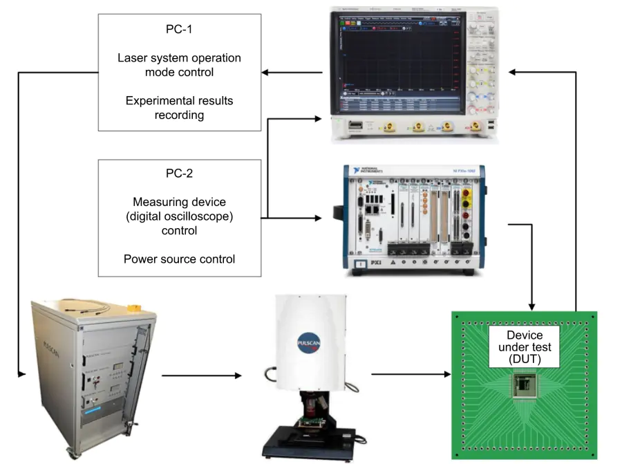
Results of focused laser irradiation of semiconductor structures having relatively small sizes of discrete components on the crystal were presented. Different laser beam depth profiles were obtained in the experiments via different lenses. The focused beam size was varied in a range of 1.4 to 3.6 μm at the beam waist. The test specimens were position-sensitive detectors with small pixel size (~15 μm). We showed that the use of different lenses with constant pulse energy and duration yields different results in sensitivity assessment. Conclusions were made as about the limitations in the application of precision irradiation methods to semiconductor structure.